Transparent Circuit Platform
A transparent flexible substrate carries the conductive paths, LED pads and external connections while preserving open viewing areas.

Bring illuminated text, numbers, symbols and simple graphics into compact products by bonding LED emitters directly onto a transparent flexible circuit.
Choose a programmable dot-matrix layout, dedicated segments or a custom-shaped LED array. The outline, emission colors and FPC connection are developed around your application.
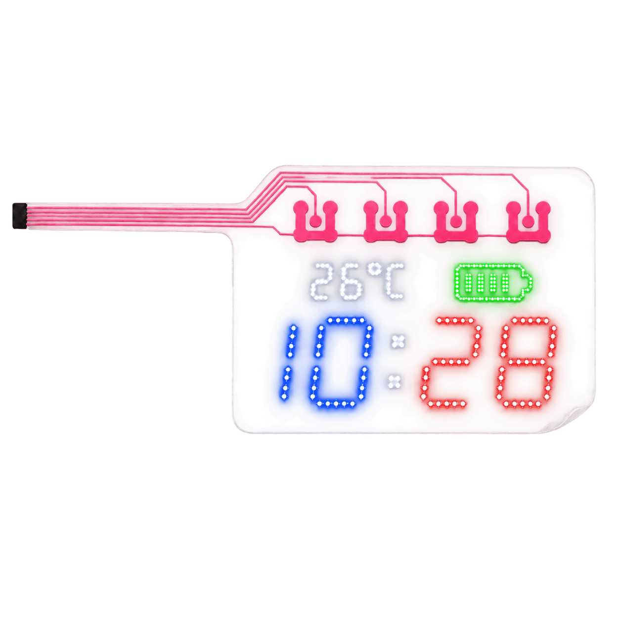
The display should fit your product: its visible window, enclosure curvature, connector position and available electronics space.
There is no fixed list of standard screen sizes in this family. A narrow format such as 60 × 15 mm can be a starting point for discussion. Circular, rectangular and irregular outlines can also be reviewed.
Final dimensions depend on the content, LED arrangement, circuit routing and assembly. We review the active display area separately from the overall outline, including the FPC tail and connection.
This product combines a transparent flexible circuit with LED emitters bonded directly onto its circuit pads and connected to suitable driving electronics. Individual LEDs generate the visible content. Clear areas between LEDs and circuit features allow the background to remain visible. The transparent film supports the circuit; it does not emit light by itself.
Passive perimeter features, conductive tracks and connection pads remain unlit. Only the specified LED elements emit light.
The innovation is in bringing established technologies together: transparent substrates, conductive circuits, protective layers, LED bonding and display driving. Integrated into one custom module, they enable transparent, flexible, small-format displays with dot-matrix, dedicated-segment or irregular layouts.
The circuit provides support and electrical connections. The bonded LEDs generate the light, and the driver selects the pixels, segments or lighting zones. Material selection, bonding, circuit routing and control are developed together around the product.
A transparent flexible substrate carries the conductive paths, LED pads and external connections while preserving open viewing areas.
Discrete LED emitters are bonded onto the circuit in the required pixel grid, segment artwork or application-specific shape.
Matched driving electronics turn the assembled circuit into a controllable display, with content and colors defined by the layout and controller.
A pixel grid for changeable text, numbers, icons and simple graphics.
Predefined characters, logos and symbols for a focused product interface.
Application-specific shapes and lighting zones for device integration.
Product images are visual references for custom layouts and emission effects. Final appearance and specifications are confirmed with the approved sample.
Change the content within a defined pixel area.
A dot-matrix design arranges LEDs into rows and columns. Selected pixels illuminate to form text, numbers, symbols and simple graphics. It is suitable for changing messages, status information and basic animation, subject to pixel count and controller capability.
Layouts down to 0.5 mm can be reviewed. Around 1.0 mm is generally a better starting point when transparency is the priority. Closer spacing increases detail but also increases LED and circuit density.
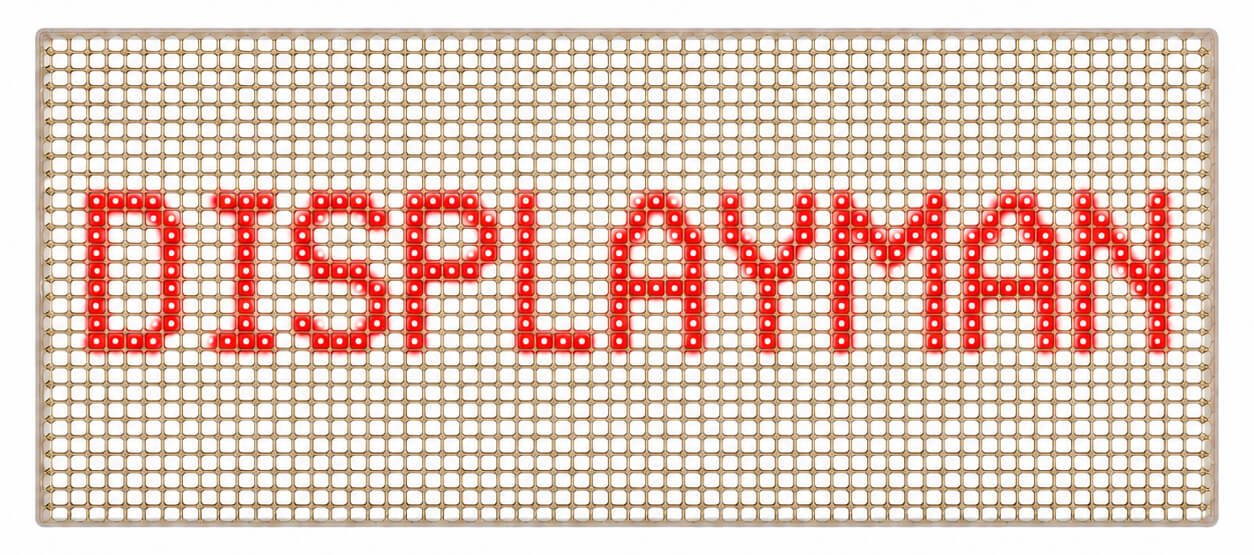
Visible LED points form changeable text on a transparent circuit. Red emission reference.
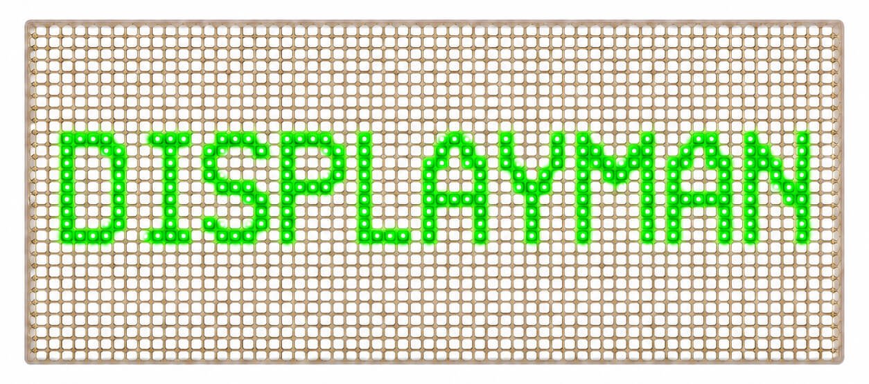
Visible LED points form changeable text on a transparent circuit. Green emission reference.
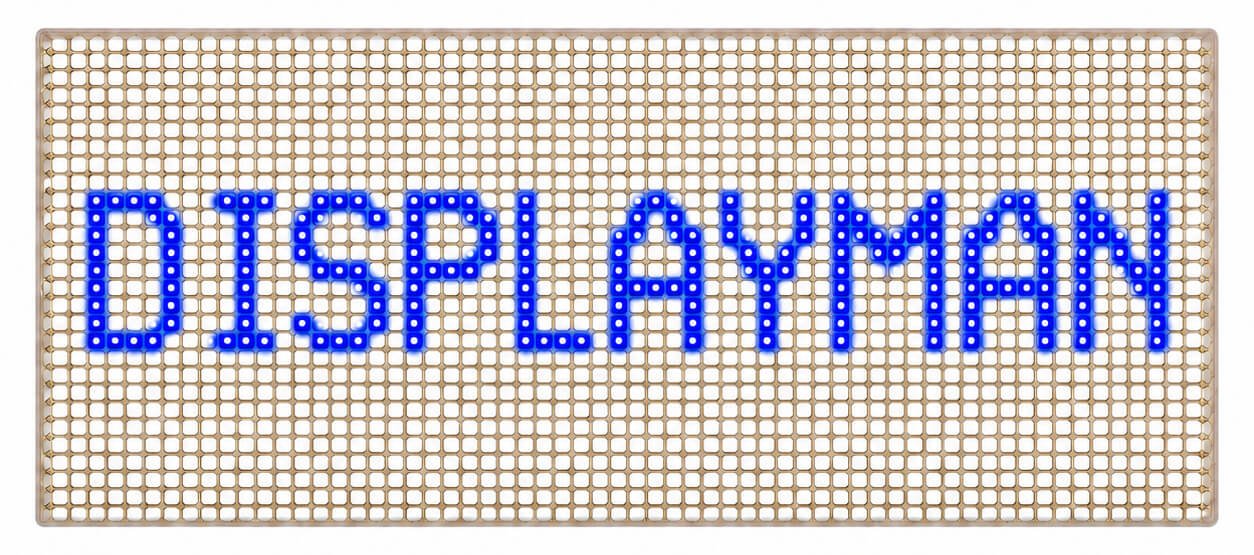
Visible LED points form changeable text on a transparent circuit. Blue emission reference.
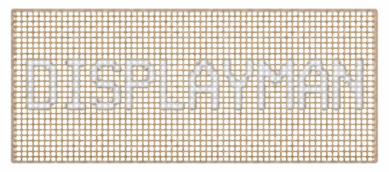
Visible LED points form changeable text on a transparent circuit. White emission reference.
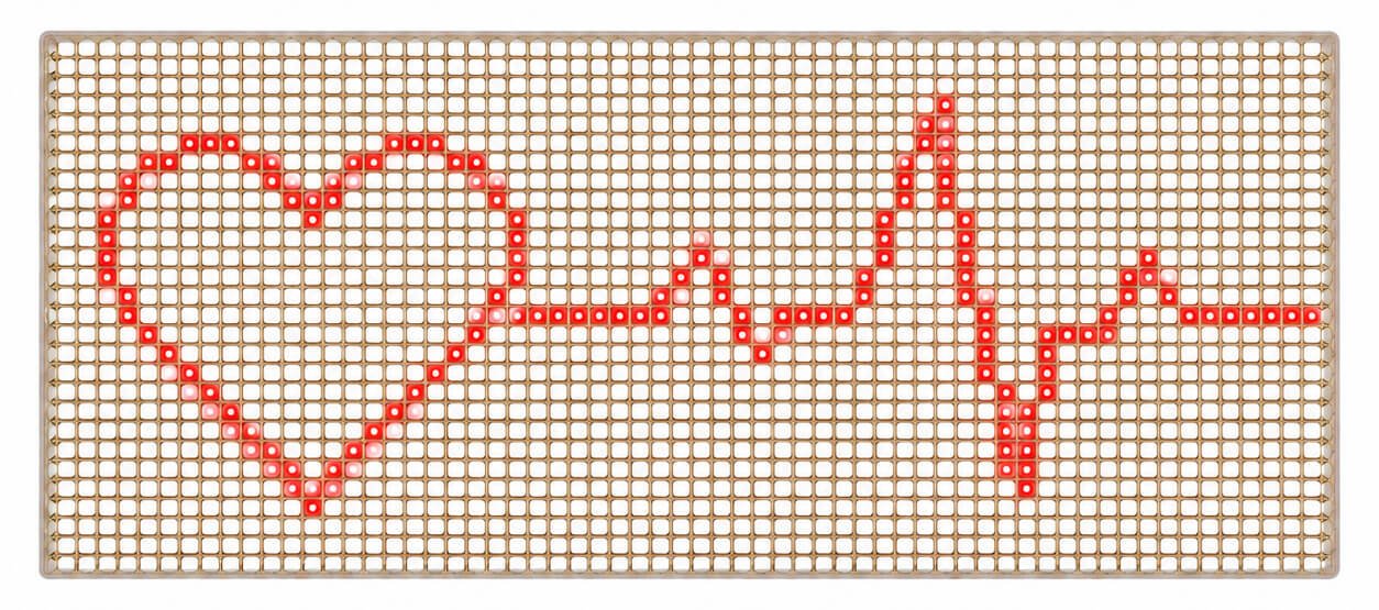
Visible LED points form simple graphics on a transparent circuit. Red emission reference.
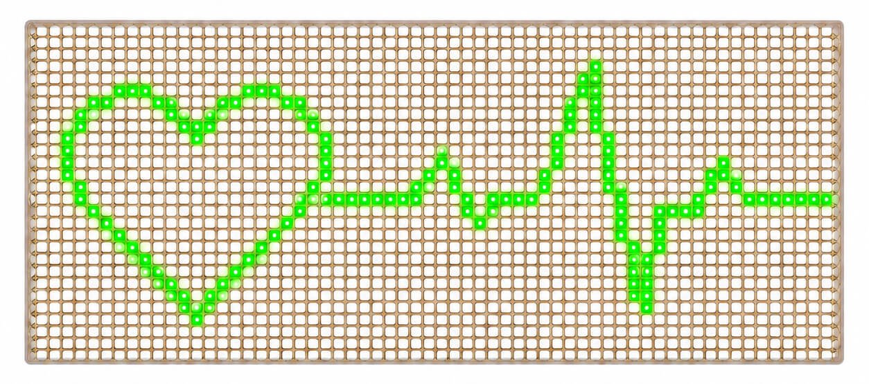
Visible LED points form simple graphics on a transparent circuit. Green emission reference.
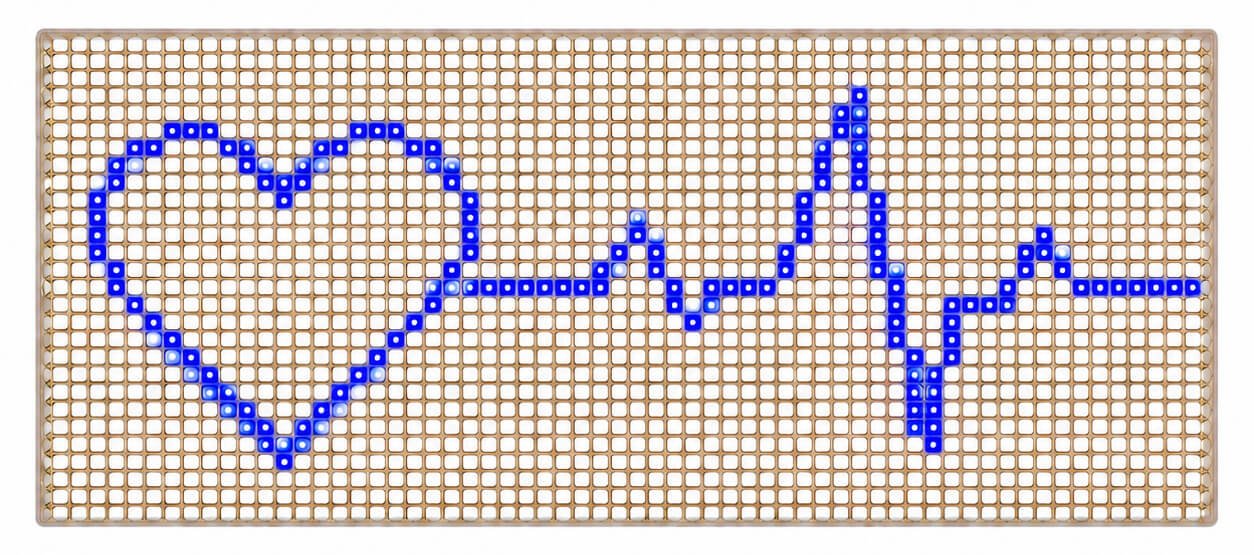
Visible LED points form simple graphics on a transparent circuit. Blue emission reference.
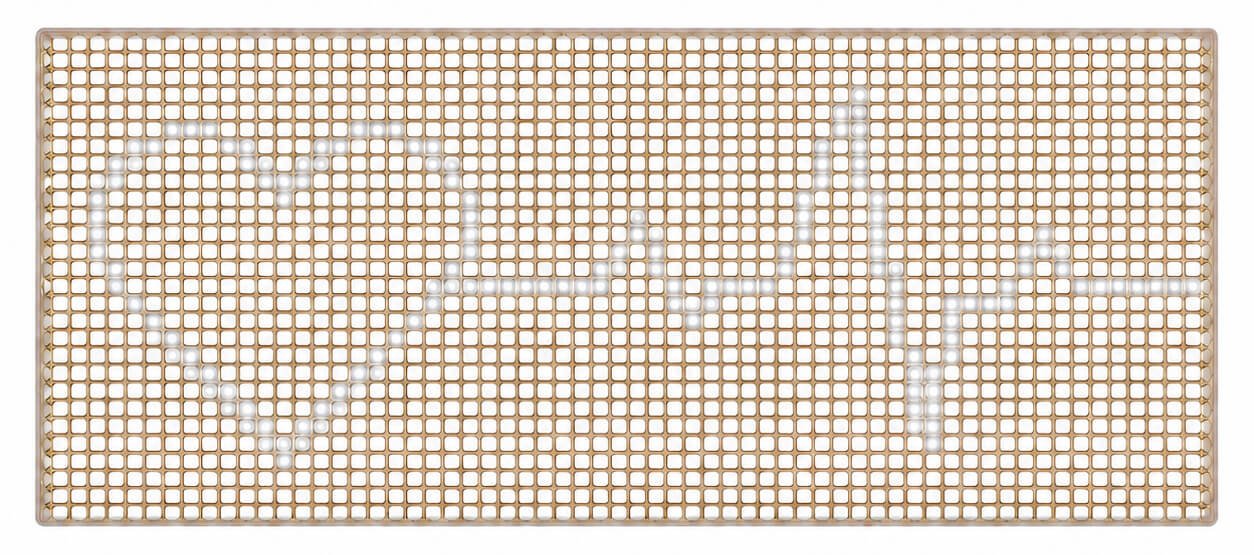
Visible LED points form simple graphics on a transparent circuit. White emission reference.
Dedicated numbers, symbols and brand elements in a layout designed for your interface.
A segment display uses predefined emitting elements. Segments can form time digits, temperature readings, battery indicators, mode symbols, warning icons or custom lettering. Each segment or group is assigned to the required control function.
In the circular examples below, only DISPLAYMAN, ON and the power symbol emit light. The outer ring and FPC routing remain unlit.
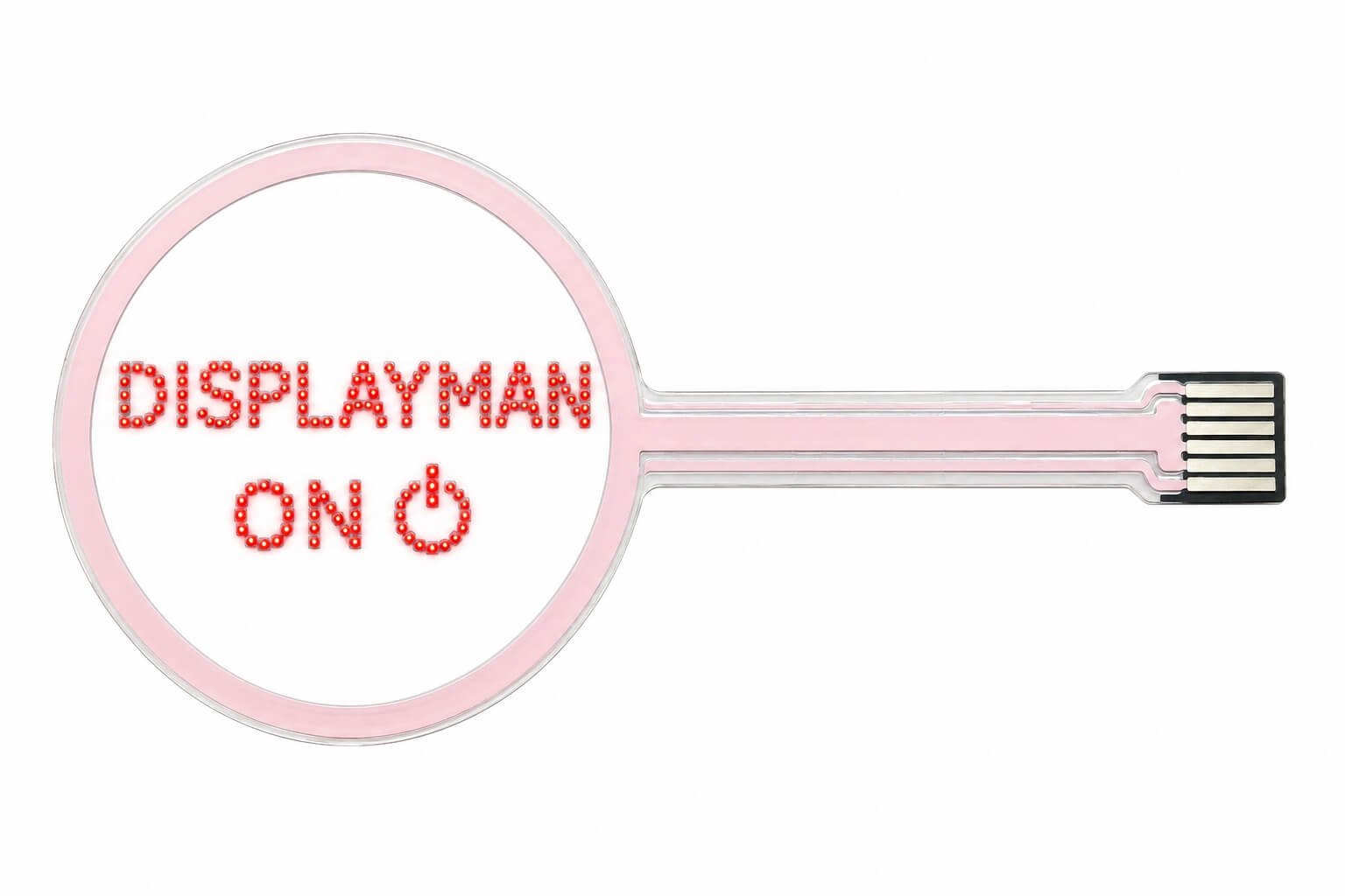
Individual LED beads form the lettering and power symbol. The passive ring and connection tracks do not emit light.
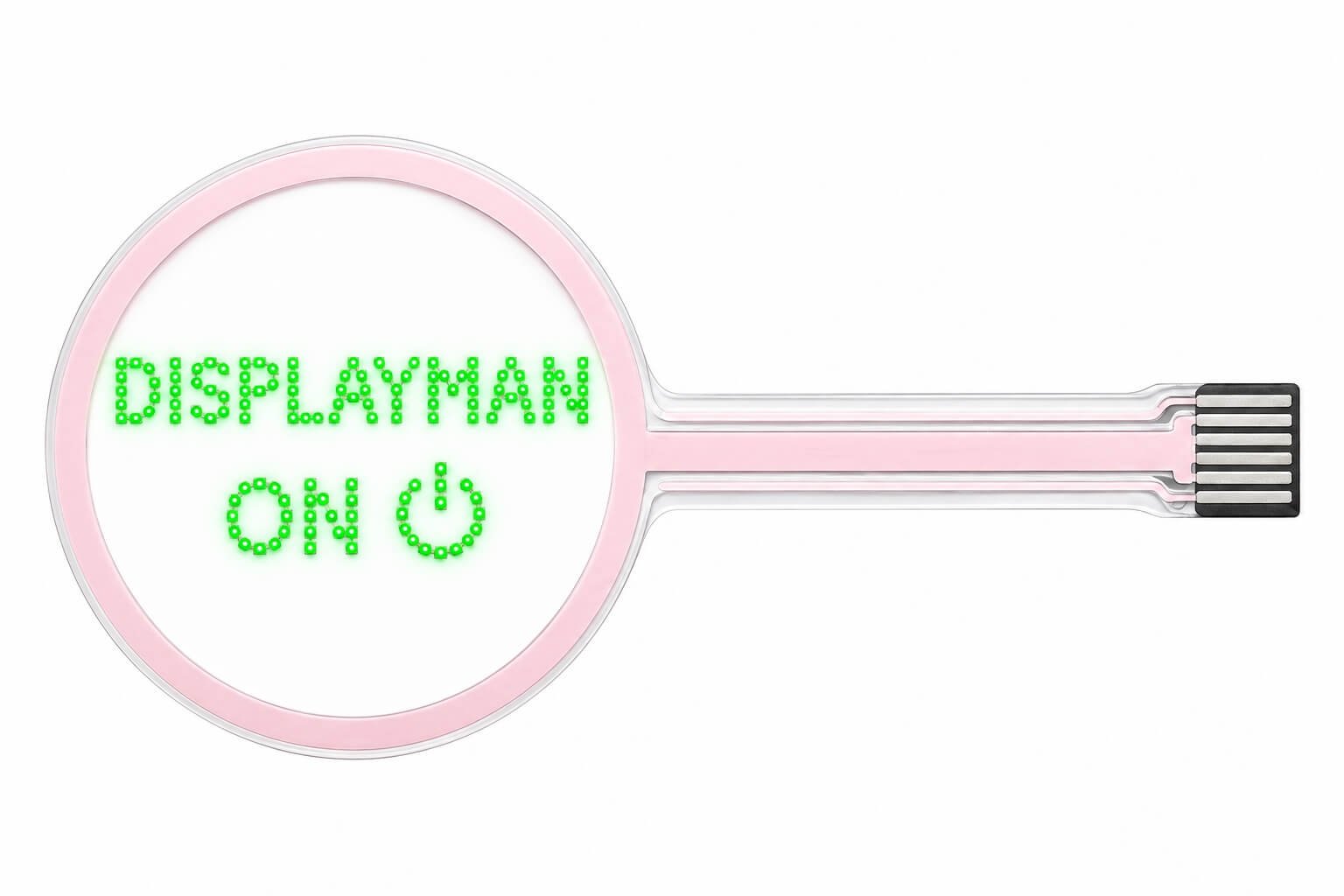
Individual LED beads form the lettering and power symbol. The passive ring and connection tracks do not emit light.
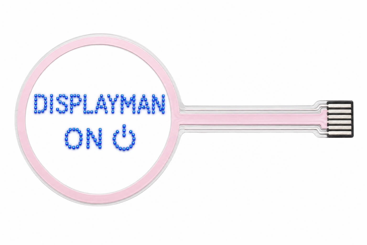
Individual LED beads form the lettering and power symbol. The passive ring and connection tracks do not emit light.
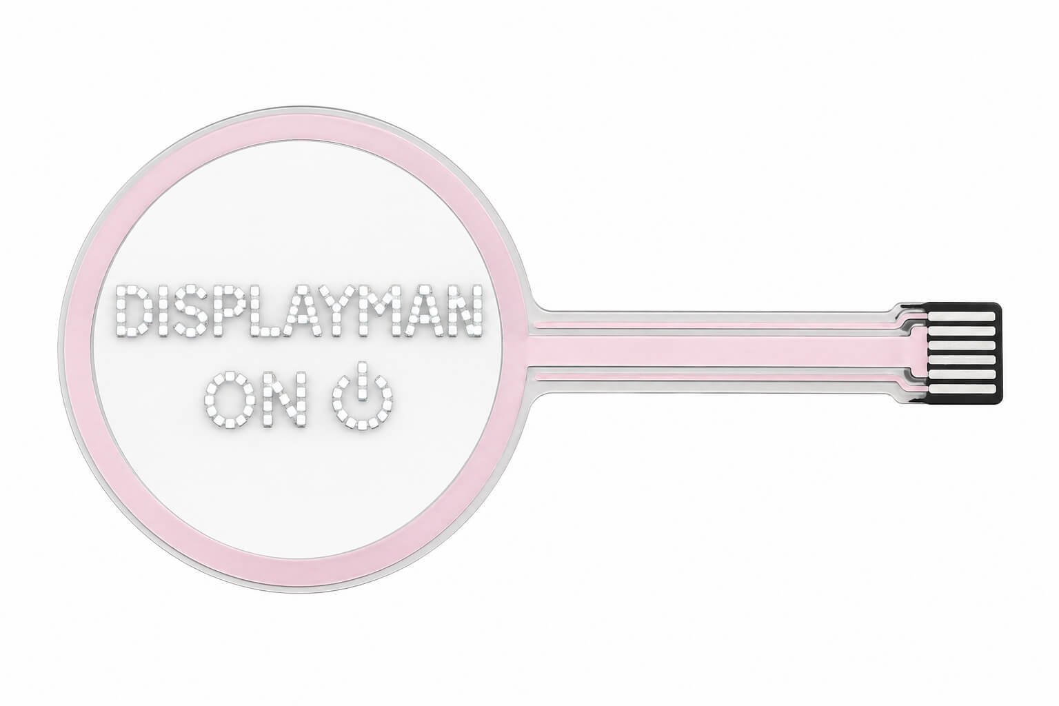
Individual LED beads form the lettering and power symbol. The passive ring and connection tracks do not emit light.
The controller changes which predefined elements are illuminated; the physical layout stays fixed. Confirm character shapes, symbol positions and independently controlled groups before finalizing the circuit. New symbols normally require a design revision.
| Configuration | Design Approach |
|---|---|
| Single Color | Red, green, blue or white emission for a consistent interface. |
| Different Colors by Zone | Assign colors to selected digits, symbols or functional areas. |
| RGB | Use suitable RGB LEDs and driving electronics for adjustable colors. |
| Dedicated White | Specify white LEDs when white emission is an important requirement. |
RGB color mixing and dedicated white LEDs are different configurations. Brightness adjustment, dimming and animation are reviewed with the selected LED packages and control system.
The transparent FPC material can have a highly clear appearance. Optical performance depends on the selected material and layer stack.
LEDs, tracks, pads, protection and bonding layers affect the finished display. Clear-film transmittance is not the same as whole-module transparency.
Evaluate the display against the intended background and ambient lighting, with its actual cover and enclosure.
LED spacing, trace routing and connector placement are reviewed together. Where practical, less-transparent connection and driver regions can sit outside the primary viewing window. Agree the measurement area and optical target for the actual assembly.
These displays use individual LED emitters. At close range, separate LEDs and their spacing remain visible. At around one meter or farther, suitably designed content can appear substantially smoother, depending on pitch, brightness and viewing conditions.
Transparent OLED uses an OLED pixel structure and emissive layers. Its close-up image appearance differs from the discrete LEDs used here. For handheld products, review samples at the intended operating distance.
The material system has three layers of engineering: the substrate, conductive circuit and protection. LED bonding and driving then turn that circuit platform into a display.
The routes below describe the broader material toolbox. They are alternatives to evaluate, not a statement that every material is present in one module. The approved design identifies the actual substrate, conductor, protective layers and bonding process.
PET and colorless polyimide (CPI) are transparent-film directions. Optical clarity, thermal limits, dimensional stability, thickness and bending behavior guide the choice. LCP may also enter the wider circuit-material discussion where electrical requirements are important; its optical suitability must be established for the specific grade.
Fine metal traces, metal mesh, ITO and silver-nanowire technologies offer different ways to combine electrical conduction and optical transmission. LED current paths, bonding pads and driver connections require particular attention: transparent-electrode materials are not automatically interchangeable with LED interconnects.
Transparent cover layers and coatings protect the circuit and connections. Transparent polyurethane (PU) and self-healing coating concepts belong in this material discussion, with compatibility and durability evaluated separately. Local reinforcement can support connectors without making the whole module rigid.
| Material / Technology Route | Role in the Material System | What Must Be Reviewed |
|---|---|---|
| PET — polyethylene terephthalate | Clear flexible substrate for a compatible circuit and LED assembly process | Film thickness, clarity, heat exposure, shrinkage and dimensional stability |
| CPI — colorless polyimide | Transparent substrate direction combining optical and thermal requirements | Actual grade, tint, cost, adhesion and compatibility with bonding and protection |
| LCP — liquid crystal polymer | Specialist circuit-material direction when electrical performance is a priority | Do not assume conventional LCP is optically clear; verify the proposed film, transparency and manufacturability |
| Fine metal traces / Metal Mesh | Patterned conductive paths with open see-through areas | Trace visibility, line geometry, current capacity, voltage drop and bond-pad design |
| ITO — indium tin oxide | Transparent conductive-oxide route for compatible electrode functions | Resistance, bending durability and electrical contact; confirm suitability for the intended LED circuit |
| AgNW — silver nanowires | Transparent conductive-network route | Uniformity, patterning, connection resistance, protection and current requirements |
| Transparent PU and protective films | Protection against handling and environmental exposure | Haze, adhesion, chemical compatibility, aging and effects on the assembled bend |
| Self-healing transparent coatings | Advanced protective-material direction for surface-damage management | Supplier evidence, process compatibility and actual recovery conditions; not a standard module feature |
Clear substrate transmission can approach 90% for a suitable material. Complete-display transparency also depends on LEDs, conductor coverage, adhesives, protection and the chosen measurement area. The display must be reviewed as an assembled system.
Material background: Kaneka transparent polyimide · TDK transparent conductive-film technologies. These references describe material technologies, not the bill of materials for a DisplayMan module.
The process integrates transparent-substrate preparation, conductive-pattern fabrication, direct LED bonding, protective assembly and driver integration. The approved material stack-up and LED layout determine the production route. Fine-pitch assembly and reliable connections matter as much as the transparency of the film.
Define the active area, dot-matrix or segment artwork, LED colors, current paths, FPC tail, connection pads and reinforcement. Review the balance between detail, transparency and routing space.
Control surface cleanliness, handling and dimensional stability before circuit processing. Review the film and adhesive temperature limits against subsequent assembly steps.
Form the specified conductors and connection features using the selected imaging and patterning process. Inspect line geometry, alignment, opens and shorts before LED placement.
Bond the individual LED emitters directly to the circuit pads using a process compatible with the selected substrate, conductor and LED package. Check polarity, placement accuracy, joint quality and the driver interface.
Apply the approved protective layers, define the custom outline and add local stiffeners. Keep bending away from sensitive joints and reinforced connector transitions.
Connect the matched driver and verify addressing of the pixels, segments or lighting zones. Test color, current, heat and uniformity. Review transmission, bend conditions and environmental requirements on the assembled sample before production approval.
A flexible substrate does not automatically make a populated display repeatedly foldable. Minimum bend radius, bend direction and cycle life are project-specific assembly requirements.
Define the installed shape before finalizing the populated circuit.
Permitted bending depends on the substrate, conductive tracks, LED placement, bonded connections, protective layers and connection structure. Review bend direction, radius, flat areas, tail routing and strain relief together.
Assembly bending and repeated flexing are different requirements. A flexible film does not automatically make the populated display suitable for repeated folding. Specify dynamic movement at the beginning of the project.
Adapt the LED outline and zones to the device structure.
Transparent flexible circuits can carry custom-shaped LED arrays for beauty-device integration. Openings, connection tails and emitting zones can be arranged around the mechanical design.
A display interface prioritizes readable information. A beauty-device array may instead prioritize LED positioning, emission distribution, zone control and thermal management.
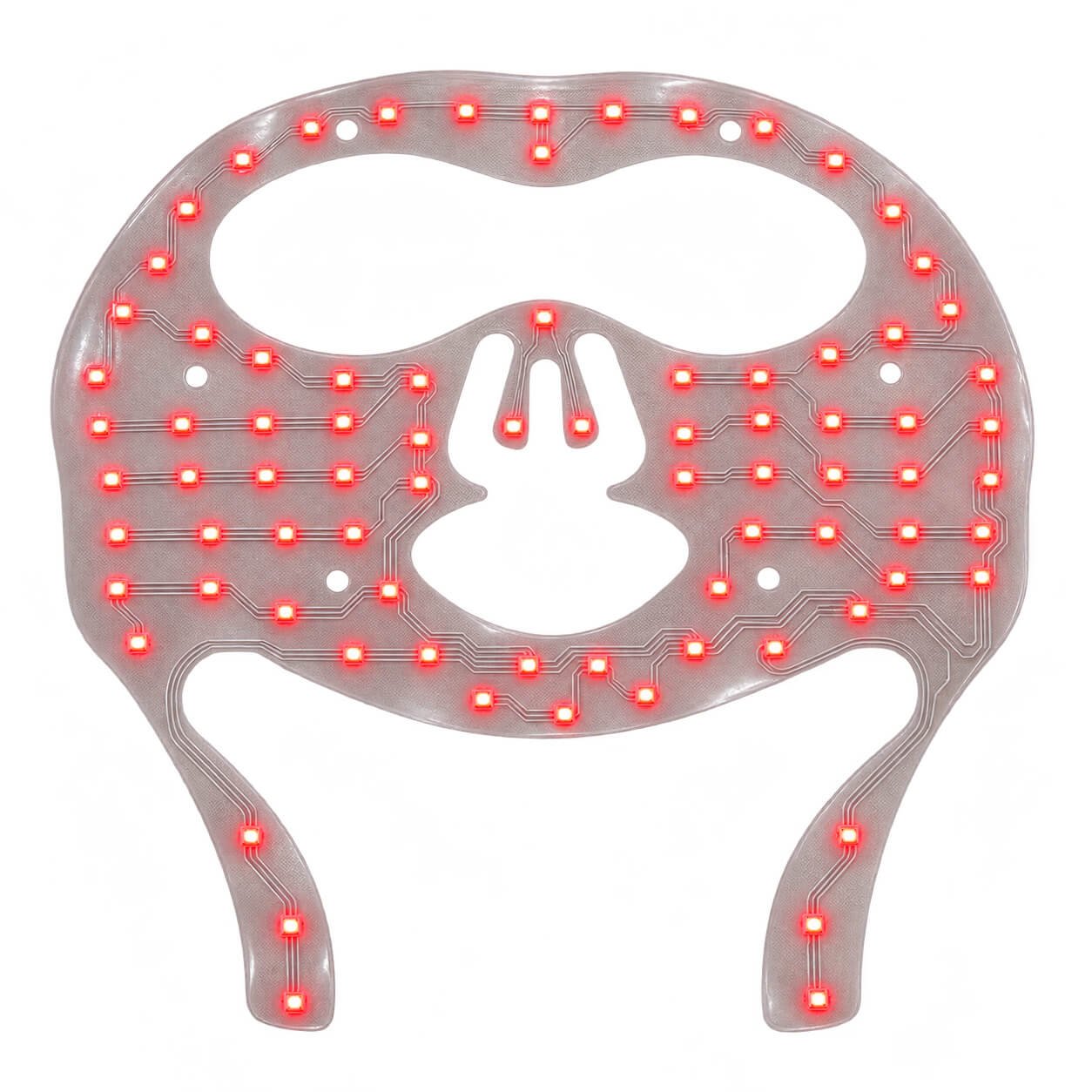
Custom-shaped transparent flexible LED array. Color-effect reference; wavelength and optical output are specified separately.
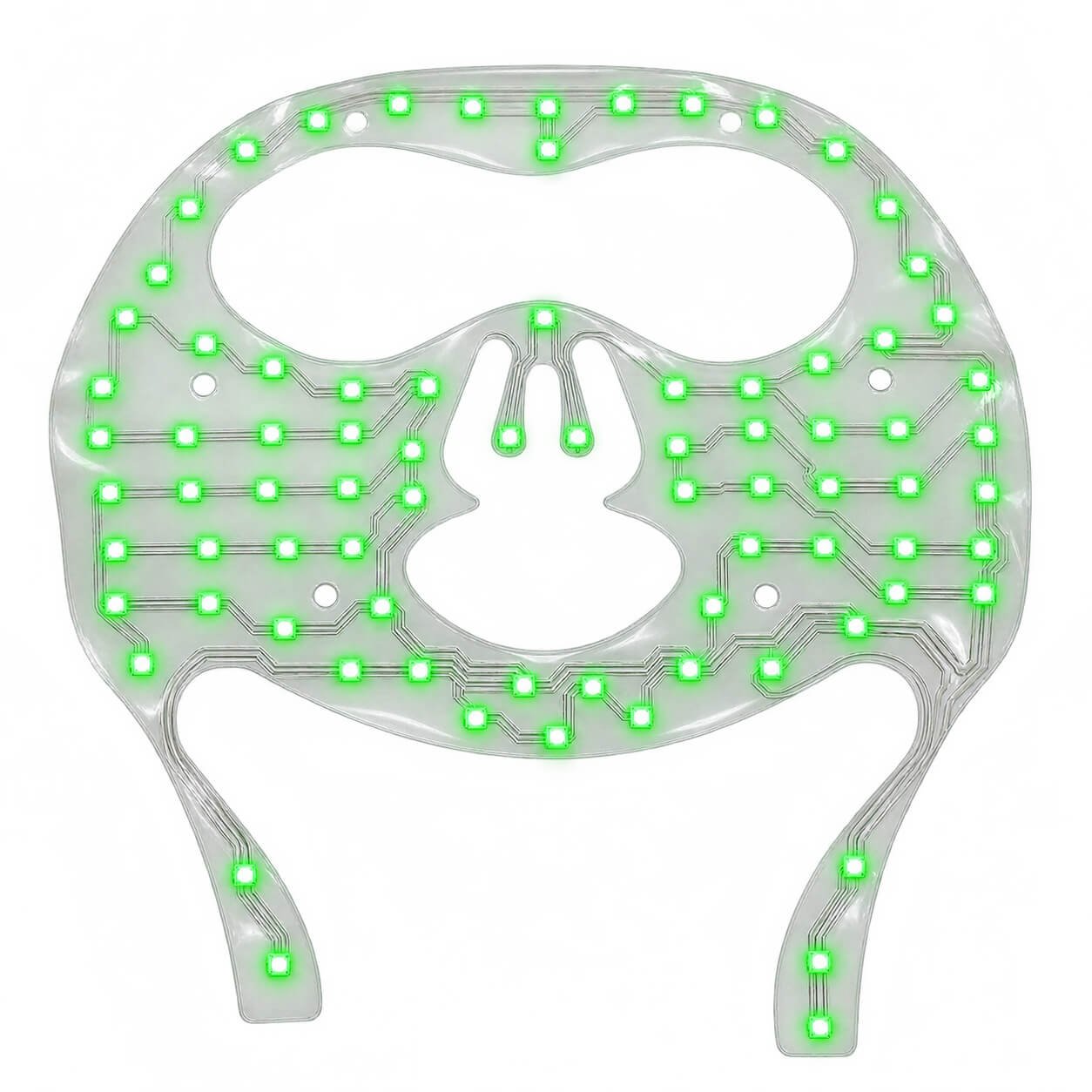
Custom-shaped transparent flexible LED array. Color-effect reference; wavelength and optical output are specified separately.
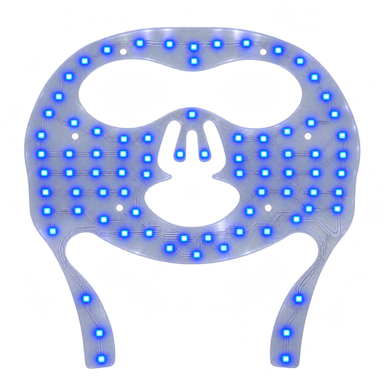
Custom-shaped transparent flexible LED array. Color-effect reference; wavelength and optical output are specified separately.
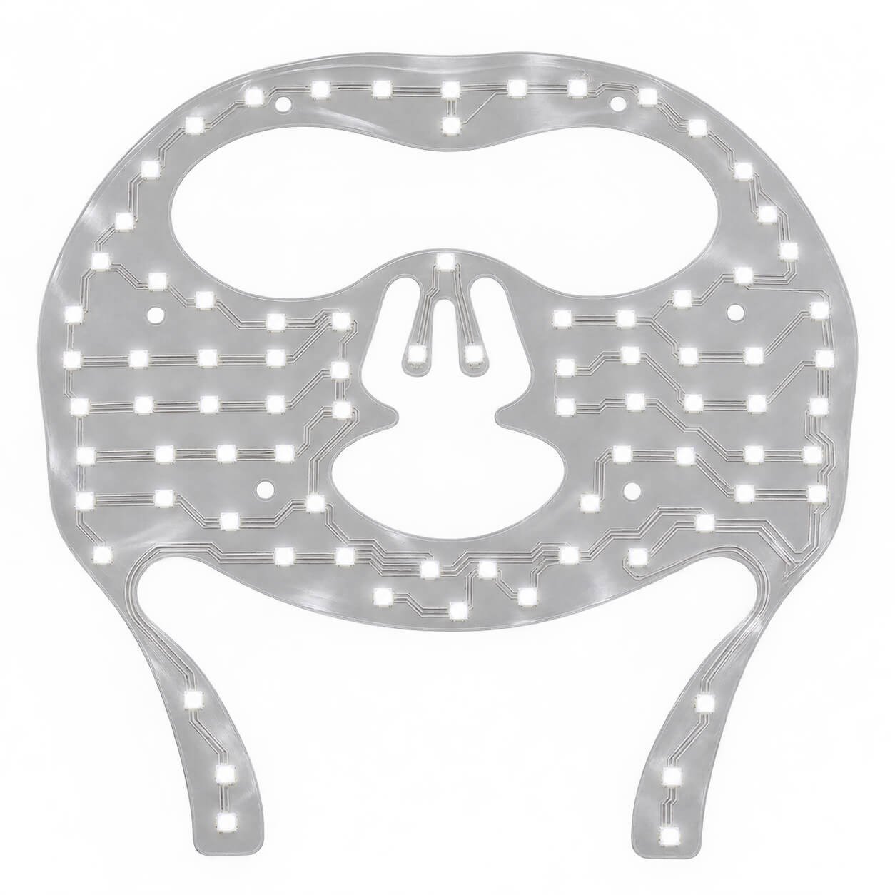
Custom-shaped transparent flexible LED array. Color-effect reference; wavelength and optical output are specified separately.
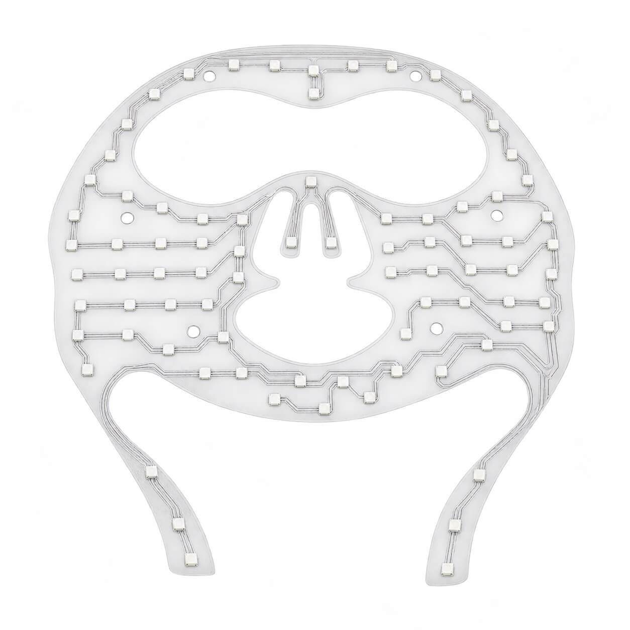
Unlit reference showing the film outline, LED positions and connection structure.
Provide the required outline, LED zones, wavelengths, optical output, uniformity, duty cycle, power and control method. Thermal behavior, encapsulation, cleaning and application-specific validation are reviewed separately. These images do not establish treatment performance.
| Item | What Can Be Reviewed |
|---|---|
| Overall Shape | Rectangular, circular, narrow strip or irregular outline. |
| Active Area | Dimensions and position of the emitting region. |
| Display Format | Dot matrix, dedicated segments or custom LED zones. |
| Pixel Pitch | Down to 0.5 mm for review; around 1.0 mm when transparency is prioritized. |
| Content | Text, digits, symbols, logos, simple graphics and lighting patterns. |
| Emission | Red, green, blue, white, RGB or different colors by zone. |
| FPC Connection | Tail length, exit direction, contact layout and connection position. |
| Control | Driver architecture, dimming, animation and host communication. |
| Mechanical Integration | Flat or approved curved mounting, protection and bonding. |
| Optical Targets | Brightness, viewing conditions and finished-module transparency. |
| Operating Conditions | Temperature, moisture, cleaning and protection requirements. |
| Commercial Requirements | Sample quantity, production volume, tooling and schedule. |
Final specifications are established for the approved design. There is no single universal brightness, thickness, voltage, maximum size or bending radius for every configuration.
Use the clear circuit where information or light must coexist with the visible product surface beneath it.
Custom-shaped LED arrays, operating indicators and treatment-zone layouts can follow the device geometry. Define wavelength, optical output, skin-contact construction and thermal behavior for the intended device; display illustrations do not establish treatment performance.
Transparent status windows, clocks, battery icons, logos and changing text can be integrated into clear covers or curved housings. Review close-viewing detail and standby appearance.
Compact numeric readouts and icons can preserve the appearance of glass or transparent covers. Match readability to the background, ambient light and cleaning conditions.
Thin shaped indicators can be reviewed around the approved bending zones. Sweat exposure, skin contact, repeated movement, power and encapsulation are product-level design requirements.
Custom indicators or decorative information layers may suit selected interior concepts. Temperature, vibration, optical readability and automotive qualification must be evaluated for the complete application.
See-through status indicators and compact information windows can be reviewed for equipment interfaces. Cleaning resistance, electrical safety and any medical qualification remain specific to the finished device.
Compare viewing distance, close-up detail and custom development needs. Flexible transparent LED can look smooth at normal viewing distances, while OLED offers finer luminous detail when viewed in the hand.
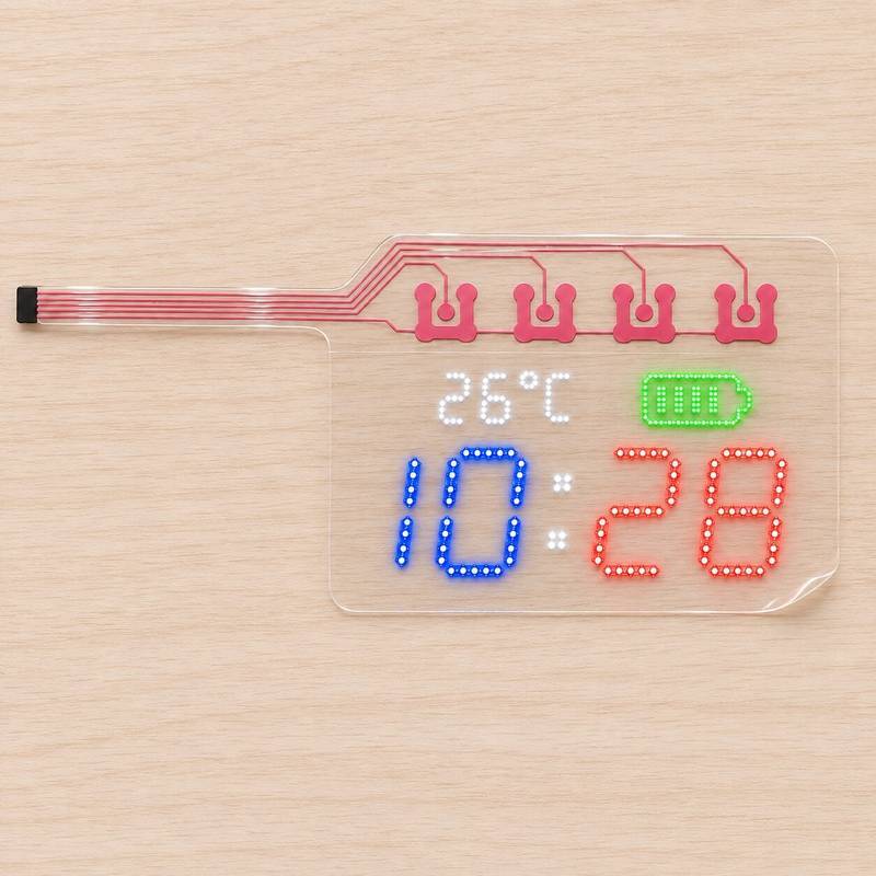
Custom dot matrix, fixed segments and shaped LED arrays with a comparatively accessible development budget.
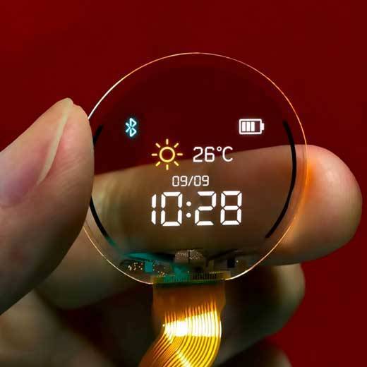
Explore smooth illuminated digits, icons and dedicated segments for premium close-viewing interfaces.
Explore Custom Transparent OLED →Individual LED points can visually blend together, making text and graphics appear smooth. Under suitable viewing conditions, the difference in perceived smoothness compared with high-density AMOLED can be difficult to notice.
At close viewing distances, flexible transparent LED reveals distinct light-emitting points and spaces between them. High-density AMOLED appears much more continuous, with individual pixels generally difficult to distinguish with the naked eye.
The distance at which LED points visually merge depends on pixel pitch, brightness, content and eyesight. This comparison concerns the perceived smoothness of text and graphics; it does not imply identical resolution, color or contrast.
| Selection Factor | Flexible Transparent LED | Custom Transparent OLED |
|---|---|---|
| Light-emitting structure | Individual LED emitters mounted on a clear flexible circuit | Patterned organic light-emitting layer; a smoother luminous surface |
| Close-viewing detail | When held in the hand, individual LED points and the gaps between them are clearly visible | Finer-looking, more continuous segment and icon edges |
| Viewing distance | At around one metre or more, LED points can visually merge and text or graphics can appear smooth; differences in perceived smoothness versus AMOLED may be difficult to notice under suitable conditions | Well suited to fine fixed information viewed at close range |
| Programmable dot matrix | Available as a custom pixel layout for changing text, icons and simple graphics | A new custom small-format dot-matrix panel requires a separate, high-investment development route |
| Practical OLED offer for these projects | Dot matrix, dedicated segments or shaped arrays | Custom segments and icons are the practical currently offered route; their physical artwork is fixed |
| Pixel pitch | Down to 0.5 mm subject to review; about 1.0 mm is a useful starting point for transparency | High-density AMOLED reference examples: approximately 44–59 μm (0.044–0.059 mm). These are not specifications for the custom transparent segment OLED shown here; its emitting shapes are defined by the panel artwork. |
| Transparency | Clear spaces between LEDs and traces; substrate transmission is different from module transparency | Depends on the panel stack, electrode pattern and emitting area; compare actual samples |
| Flexibility | Clear flexible carrier with assembly-specific bend limits | The referenced custom glass OLED construction should not be assumed flexible |
| Colors | Red, green, blue, white, selected zones or RGB depending on the LED and driving design | Emission colors and zones depend on the custom OLED process; confirm feasibility |
| Custom dot-matrix development / tooling reference | Approximately USD 4,000–5,000 | Approximately USD 4–5 million for a new custom dot-matrix panel development |
| Unit-price positioning | Generally the lower-cost direction for the compact custom projects discussed here; quoted by design and quantity | Premium direction when fine luminous detail justifies the cost; quote segments separately |
| Best starting point | Changing content, flexible outlines and a manageable custom development budget | Refined fixed icons and numbers on a premium transparent interface |
AMOLED reference: Samsung lists 432 PPI and 577 PPI for two Super AMOLED panels. Using pixel pitch = 25,400 ÷ PPI gives approximately 58.8 μm and 44.0 μm respectively. These are pixel-centre spacing examples, not LED package sizes or specifications for our custom transparent segment OLED. Source: Samsung Global Newsroom →
DisplayMan’s indicative project references are USD 4,000–5,000 for custom LED dot-matrix development versus USD 4–5 million for a new custom transparent OLED dot-matrix panel. Comparing the corresponding endpoints gives approximately 1,000×. These are different development scopes, not identical tooling packages or a unit-price ratio. The OLED figure does not apply to custom segment OLED tooling. Scope, electronics, validation, quantity and quotation must be confirmed for each project.
Describe the product, installation, viewing distance and operating environment.
Provide text, symbols or graphics. Identify independently controlled elements for segment designs.
Confirm the display window, total outline, FPC tail, connector and curvature.
Define color, brightness targets, power, control behavior and operating conditions.
Approve the drawing, then evaluate samples in the intended enclosure.
Agree appearance, functions, assembly requirements and inspection criteria.
Overall dimensions, active area, drawing or sketch, openings, mounting, curvature and FPC exit.
Exact content, format, colors, viewing distance, ambient lighting, power and host-controller requirements.
Prototype quantity, production forecast, target schedule, destination market and required compliance conditions.
The innovation is the integration and productization of established technologies: transparent substrates, conductive circuits, protection, direct LED bonding and display driving. Their coordinated design enables custom small-format transparent flexible displays with dot-matrix, dedicated-segment and irregular layouts.
Flexible transparent LED uses discrete emitters and supports custom dot matrix, segments and shaped arrays. The practical small-size transparent OLED offer is dedicated segments and icons with a smoother luminous appearance. A new custom OLED dot-matrix panel is a separate high-investment development.
DisplayMan’s indicative references are USD 4,000–5,000 for custom LED dot-matrix development and USD 4–5 million for a new custom transparent OLED dot-matrix panel, approximately 1,000 times at corresponding endpoints. These are different development scopes, not unit prices. Segment OLED tooling is separate; all costs require a project quotation.
The transparent flexible circuit combines a substrate, conductive pattern and protection. PET, CPI and other specialist material routes are evaluated for the design rather than prescribed universally. LED emitters are bonded directly onto the circuit and connected to a matched driver. Only the LEDs emit light; the passive substrate and traces remain unlit.
This family is fully custom. The outline, active area, LED layout and FPC connection are developed around the application rather than selected from a fixed size list.
A format around 60 × 15 mm can be reviewed. Feasibility depends on the content, LED package, pitch, routing and connection requirements.
The practical size is confirmed through engineering review. Send the required outline and active area. A fixed maximum is not specified for this custom family.
Dot matrix uses a pixel grid for changeable content. A segment display uses predefined emitting elements for specific characters, symbols or logos. Its physical layout stays fixed.
Custom dot-matrix layouts down to 0.5 mm can be reviewed. Around 1.0 mm is generally a better starting point when transparency is the main priority.
Clear substrate transmittance and completed-display transparency are different measurements. LEDs, tracks, protection and the final assembly affect the result. Agree the requirement for the actual module and measurement area.
No. Passive rings, conductive tracks and connection pads do not emit light. Only the specified LEDs illuminate. An illuminated ring would require a separate LED layout.
No. The approximately 44–59 μm figures are calculated from published high-density Super AMOLED examples. The custom small-size transparent OLED shown here uses dedicated segment artwork; these AMOLED figures are not its product specifications. Confirm the emitting pattern and dimensions from the approved panel drawing.
Yes. When the display is held in your hand, individual LED points and the gaps between them are clearly visible. At around one metre or more, the points can visually merge and text or graphics can appear smooth. Under suitable conditions, the difference in perceived smoothness compared with high-density AMOLED can be difficult to notice. The result depends on pitch, brightness, content and eyesight.
Designs can use individual red, green, blue or white emission, different colors by zone, or RGB operation. Dedicated white LEDs and RGB color mixing require different configuration decisions.
Dot-matrix designs can support changing graphics or animation when pixel count and controller capability allow it. Video suitability depends on resolution and refresh performance. Segment displays illuminate predefined content.
Approved bending may be possible within the assembled display’s mechanical limits. Repeated folding is a separate requirement and must be evaluated during development.
Custom-shaped LED arrays can be reviewed for beauty-device integration. Define the outline, wavelength, optical output, control, thermal behavior and validation requirements.
The bare display requires suitable driving electronics. HDMI input, USB communication or another interface is a controller-level requirement to specify during development.
These depend on the custom design, electronics, sample requirements and production quantity. A project-specific quotation follows review of the application and drawing.
Share your outline drawing, display content and expected quantity. DisplayMan will review the dot-matrix, segment or custom-array approach, together with the emission colors, transparent circuit layout, FPC connection and integration requirements.
For an engineering review, please include your outline dimensions, display artwork, emission colors, FPC requirements, quantity and project schedule.
