Quick answer
How Are OLED Displays Manufactured?
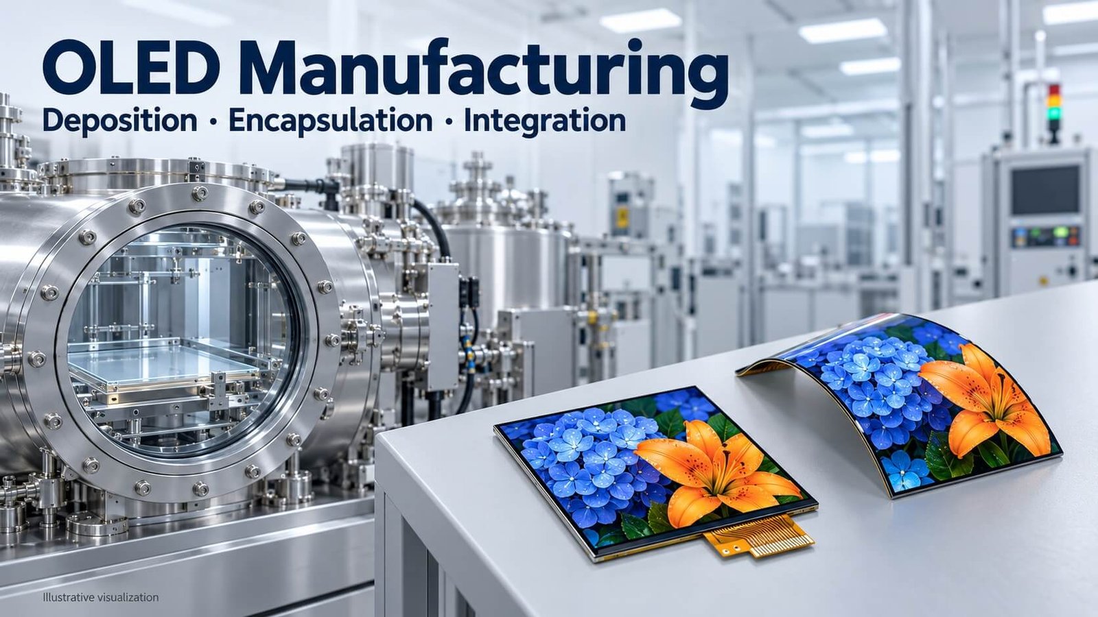
OLED manufacturing builds an electrically driven organic light-emitting stack on a prepared substrate, then adds electrodes, encapsulation and module connections. AMOLED also requires an active-matrix TFT backplane. Deposition, pixel patterning and environmental protection are central manufacturing tasks; the exact sequence depends on the panel architecture.
For an OEM project, the practical question is which available panel platform meets the display, mechanical and supply requirements. A custom FPC, touch assembly or enclosure is a different scope from developing a new OLED panel.
DisplayMan uses this distinction to help customers review AMOLED, flexible OLED and transparent OLED projects before quotation.
OLED Structure and Light-Emitting Principle
OLED stands for organic light-emitting diode. Its organic layers generate light when a driving voltage injects electrons and holes from opposite electrodes. Their recombination creates excited states; radiative relaxation releases photons. Other relaxation pathways release energy without useful light, so charge balance and emitter design matter.
The original article’s central idea remains useful: an OLED is an electrically driven light-emitting stack rather than a liquid-crystal light valve. However, the organic stack is only one part of a display. A usable module also needs addressing, encapsulation, electrical connections, mechanical support and, where specified, touch and cover glass.
A simplified multilayer device can contain the following elements. Real designs may combine functions or add further transport, blocking or charge-generation layers.
| Element | Main function | Why it matters to the finished product |
|---|---|---|
| Substrate | Supports the device on glass or a suitable flexible material | Influences mechanical construction and handling |
| Anode and cathode | Inject holes and electrons | Electrode resistance and optical properties affect operation |
| Hole injection/transport layers | Assist hole injection and transport | Help balance carrier delivery |
| Emissive layer | Converts electrical excitation into light | Influences color, efficiency and aging behavior |
| Electron transport/injection layers | Assist electron delivery | Help manage injection and recombination |
| Encapsulation | Restricts moisture and oxygen entry | Protects vulnerable organic layers and electrodes |
HOMO and LUMO describe relevant molecular energy levels for charge transport. The energy alignment between layers affects injection barriers and carrier confinement. Buyers do not normally need to specify these molecular levels; they need the resulting brightness, color, power and lifetime data for the actual panel.
OLED Panel Manufacturing: The Main Stages
There is no single process recipe for every OLED. PMOLED, rigid AMOLED, flexible AMOLED and different color architectures require different equipment and sequences. The following is a general framework, rather than a factory operating instruction. Canon Tokki provides a flexible-panel process example, while Samsung Display describes the transition from TFT processing, evaporation and encapsulation to an OLED cell. [1][2]
| Stage | What happens | Practical quality concern |
|---|---|---|
| Substrate and addressing preparation | Prepare support, electrodes and, for AMOLED, the TFT backplane | Surface quality, electrical defects and dimensional stability |
| Cleaning and surface preparation | Remove contamination and prepare interfaces | Particles and inconsistent interfaces can create defects |
| Organic layer formation | Deposit the required functional films | Thickness, composition and uniformity |
| Patterning and electrode formation | Define the required pixels and electrical paths | Alignment, short circuits and unwanted leakage |
| Encapsulation | Form the barrier and seal system | Moisture ingress, edge integrity and mechanical damage |
| Cell separation and module assembly | Separate cells and add interconnections and supporting components | Edge damage, bonding quality and mechanical stress |
| Inspection and validation | Check electrical, optical and relevant reliability characteristics | Defined acceptance conditions and repeatable measurements |
These stages explain why removing an LCD backlight does not automatically make OLED manufacturing simpler or cheaper. A thin optical stack can still depend on complex fabrication and strict process control.
For the technology’s development milestones, see OLED History. This guide focuses on manufacturing choices and their implications for product selection.
Substrate Cleaning and Surface Preparation
The original discussion of ITO preparation addresses an important point: the surface beneath an organic film affects the device built on it. Conductive films, patterned electrodes and other interfaces need controlled cleanliness and surface condition. Depending on the structure, preparation can include wet cleaning, plasma treatment or ultraviolet/ozone treatment.
ITO is a familiar transparent conductive material, but it should not be treated as the mandatory electrode in every OLED architecture. Electrode design also depends on whether light exits through the substrate, through the upper electrode, or through a transparent structure.
Particles can interfere with thin films or create local electrical defects. Residues and unsuitable surface treatment can affect film formation and injection. Treatment parameters must therefore belong to a qualified process; a general article should not prescribe one acid mixture, plasma exposure or roughness target for all panels.
For module integration, the useful implication is straightforward: keep display surfaces, exposed connections and bonding areas protected. Follow the module supplier’s cleaning and handling instructions rather than applying panel-fabrication cleaning methods to a finished screen.
Vacuum Deposition and Pixel Patterning
Vacuum thermal evaporation heats suitable materials in a controlled vacuum so that vapor reaches the substrate and forms thin films. Different functional layers are built in sequence. The process must control material delivery, deposition rate, thickness and contamination.
For an RGB evaporation route, masks and alignment systems can define where particular emissive materials land. Canon Tokki describes deposition with RGB patterning and identifies precise alignment as part of its equipment technology. This is one manufacturing route, not a description of every OLED panel. [3]
Fine-pattern alignment becomes demanding when subpixels are small or the deposition area increases. The physical behavior of masks, substrates and deposited material must be controlled together. A quoted pixel resolution is therefore connected to the panel’s established manufacturing platform, not simply a software setting that can be changed for an individual order.
The original article included specific vacuum pressures and deposition rates. Those numbers are not retained as universal specifications: suitable conditions depend on equipment, materials, device structure and the qualified process window.
OEM implication: asking for a new active area, pixel count or subpixel structure may require a new panel development program. It is a different request from changing an FPC, controller board or cover glass around an existing panel.
Solution Processing, Inkjet Printing and Transfer Methods
The original article correctly identified that organic films can be formed by more than one technique. These alternatives should be explained without assuming that every method is interchangeable or commercially available for every product.
Spin coating
Spin coating spreads a solution across a rotating substrate. Film formation depends on the solution, rotation and drying conditions. It is useful for material and device development and selected coating tasks, but it does not by itself solve the selective placement of fine RGB subpixels. Avoid the absolute claim that it can never be part of a production process.
Inkjet printing
Inkjet systems place controlled droplets at selected locations. Ink formulation, droplet behavior, placement accuracy and drying must work together to produce the required film. Printing an organic encapsulation layer is also a different task from printing the emissive RGB material. Kateeva’s equipment information illustrates inkjet applications in OLED thin-film encapsulation. [4]
Laser transfer and other approaches
Laser-assisted transfer uses a donor structure and controlled energy delivery to transfer material onto a receiving substrate. It is a process option discussed in OLED development, rather than an automatic upgrade for any panel. Other approaches include organic vapor jet printing; UDC describes OVJP as a solvent-free, mask-free deposition platform. Its equipment and commercial readiness must be evaluated for the intended product. [5]
The buying question is not “Which method sounds newest?” It is “Which qualified panel platform meets the project requirements and supply plan?”
How OLED Displays Produce Color
The original article’s three color categories are worth retaining. They describe different ways to obtain the red, green and blue contributions needed for full-color images.
| Architecture | Basic approach | Selection consideration |
|---|---|---|
| Direct RGB emission | Pattern red, green and blue emissive regions | Review the actual subpixel layout, resolution and color performance |
| White OLED with color filters | Generate a broad light spectrum and filter it into color channels | Evaluate the complete optical stack and measured efficiency |
| OLED with color conversion | Convert part of the source light into other colors | Review conversion performance, optical design and panel specification |
Samsung Display’s QD-OLED explanation is an example of an OLED source used with quantum-dot color conversion. It should not be confused with a quantum-dot-enhanced LCD backlight. [6]
No universal fraction of light loss, fixed emitter lifetime or single “best” color route applies to all products. Published results belong to particular materials, architectures and test conditions. The purchased display should be assessed through its own datasheet and sample measurements.
Similarly, fluorescent and phosphorescent emitters use different excitation pathways, but a theoretical internal-efficiency limit is not the same as useful light leaving a finished panel. Optical extraction, electrical losses and the operating point remain relevant.
Encapsulation: Why Moisture Protection Matters
OLED organic materials and electrodes need protection from moisture and oxygen. Encapsulation is therefore part of the panel’s functional design, not merely the outer enclosure. Samsung Display explains both rigid-panel sealing and flexible thin-film encapsulation; UDC also describes barrier technology for flexible devices. [7][8]
Rigid OLEDs can use a cover and perimeter sealing arrangement. Flexible structures need barriers compatible with their mechanical design; thin-film encapsulation can use alternating inorganic and organic layers. The exact layer stack and edge design vary.
Damaged barriers or seals can allow degradation, including non-emitting regions. A cosmetic cover, protective film or metal housing does not automatically replace the panel’s encapsulation system.
For OEM assembly, keep loads away from vulnerable edges, protect cable transitions and use approved adhesives and support structures. If outdoor use, cleaning chemicals or humidity exposure are expected, validate the complete assembly under the intended conditions. Panel encapsulation alone does not establish an enclosure’s ingress-protection rating.
PMOLED, AMOLED and Segment Displays
PMOLED and AMOLED describe addressing architectures. Segment and dot-matrix describe how information is laid out. Keeping these terms separate avoids confusing an early OLED format with the whole technology.
A custom segment OLED uses predefined symbols or shapes and can use direct segment addressing. A passive-matrix OLED typically uses crossing row and column electrodes; selected intersections emit as the driver scans the matrix. As the multiplex ratio changes, duty cycle and peak driving requirements become important. Resolution, brightness, power and aging must be balanced within the driver and panel limits.
AMOLED uses a TFT backplane with pixel circuits that control emission. A two-transistor/one-capacitor circuit is a basic teaching example, not a universal commercial design. Practical compensation circuits can use additional devices to manage variation and aging. AMOLED operation can also involve emission timing or modulation, so “there is no duty-cycle issue” is too absolute.
| Project requirement | Product direction to investigate | Check before committing |
|---|---|---|
| Fixed symbols or a dedicated status interface | Custom segment OLED where feasible | Artwork, driver approach, tooling and production quantity |
| Compact text, icons or simple graphics | PMOLED displays | Available matrix, multiplex limits, interface and content |
| Detailed full-color graphics or video | AMOLED displays | Resolution, host compatibility, timing, power and software |
The architectural advantage of AMOLED does not make it a drop-in replacement for an existing PMOLED. Mechanical fit, driver electronics, initialization and host software may all change. For a dedicated comparison, see AMOLED vs PMOLED.
Flexible OLED: Manufacturing Capability and Integration Limits
A flexible OLED combines an appropriate substrate, thin-film device structure, barriers and interconnections. Flexibility is a property of the complete qualified construction; a thin emissive layer does not make every finished OLED bendable. UDC discusses OLED fabrication on non-rigid substrates such as plastic and metal foil. [9]
DisplayMan’s flexible OLED direction is bendable or curvable integration. Do not assume repeated folding capability. A panel intended to be formed once into a supported curve is different from a display qualified for repeated bending cycles.
For a curved assembly, specify the bend axis, minimum radius, final mounting shape, support and cable exit. Confirm whether the radius refers to the active display, an inactive edge or an FPC region. These zones can have different limits.
Touch layers, cover materials, adhesives and a rigid support can change what the final assembly can tolerate. Review the stack as a whole before freezing enclosure geometry. See Flexible OLED Displays for the product direction.
Transparent OLED: A Different Optical Requirement
A transparent OLED must support both image emission and transmission of the scene behind it. The pixel arrangement, electrodes, addressing structure and optical layers must be designed for that purpose. Removing the housing from a conventional OLED does not turn it into a transparent panel.
For a customer project, transparency is only one part of the specification. Background brightness and objects behind the display affect perceived contrast. A black image area can appear as a view through the screen rather than an opaque black surface. Content should be designed with that behavior in mind.
Practical project review should include:
- Available panel size, active area, outline and mounting constraints.
- Ambient light and the brightness of the scene behind the panel.
- Content legibility at the intended viewing distance.
- Controller location, cable routing and service access.
- Touch and protective-glass requirements, including their optical effect.
- Operating schedule, static graphics and image-retention management.
DisplayMan’s Transparent OLED Displays page covers product and integration directions. For an enclosed showcase, also review Transparent OLED Display Cabinets. For operating precautions, see the OLED burn-in guide.
What Can Be Customized for an OEM Project?
Panel fabrication, module customization and system integration are different levels of work. Separating them at the RFQ stage helps establish a realistic budget and schedule.
| Development level | Typical scope | What to establish first |
|---|---|---|
| Existing module selection | Choose an available panel and driver configuration | Sample availability, interface and supply status |
| Module-level engineering | Review FPC, connector, touch, cover glass or bonding where feasible | Panel restrictions, drawings, tooling and quantity |
| System integration | Add controller, enclosure, mounting and application-specific functions | Signal source, installation and operating environment |
| New panel development | Change active area, pixel design, electrode layout or device platform | Fabrication feasibility, investment, MOQ and qualification plan |
A standard panel may remain the most practical starting point even when the final product looks highly customized. Changing a cover-glass outline does not change the panel’s active area. Likewise, a custom controller does not remove restrictions imposed by the OLED driver and electrical interface.
For quotation, provide the application, display content, preferred dimensions, expected order quantity and annual volume. Add interface details, mechanical drawings, touch requirements, operating temperature, lighting conditions and the required schedule. State which requirements are mandatory and which can be adjusted around an available module.
DisplayMan can review product selection and integration feasibility around suitable OLED options. New panel development requires a separate technical and commercial assessment; it should not be assumed from the availability of module customization.
Quality Checks Before Sample Approval
The original article focused on fabrication physics. For an OEM buyer, that knowledge becomes useful when it leads to an agreed acceptance plan.
Optical checks: assess full-field colors, gray levels, uniformity, visible defects and readability with representative content. Define brightness settings and ambient lighting so that results are comparable. For transparent screens, include the real background or a representative setup.
Electrical checks: verify power rails, current consumption with different content, startup/shutdown sequence, interface timing and host compatibility. A matching connector is not sufficient proof of electrical compatibility.
Mechanical checks: compare active area and outline dimensions with the enclosure drawing; review supports, cable routing and assembly stress. Flexible displays need their permitted curvature documented.
Reliability checks: agree on relevant temperature, humidity, operating-duration and content conditions, and define failure criteria. Accelerated testing and lifetime claims require stated methods; they should not be converted into a universal guarantee.
Keep an approved sample, agreed drawing revision and inspection criteria together. This makes later production checks more useful than judging every shipment against a product photograph.
Frequently Asked Questions
Is OLED always cheaper to manufacture than LCD?
No. Compare the actual product and order conditions. Size, backplane, deposition, encapsulation, yield, volume and supply arrangements influence cost. The old claim that OLED universally costs only 30–40% as much as TFT-LCD is not a reliable buying rule.
Are all OLED panels flexible?
No. Rigid and flexible structures have different mechanical designs. A flexible module still has specified bend limits and may be intended only for a supported curve.
Can an existing OLED panel be cut to a new size?
Do not treat a finished OLED as cuttable stock. Cutting can destroy active circuitry or encapsulation. A different active area normally requires selecting another panel or assessing new panel development.
Does OLED always consume less power than LCD?
No. OLED power varies with displayed content, brightness and device design. Compare representative operating conditions rather than assuming that removing a backlight guarantees lower system consumption.
Does encapsulation prevent burn-in?
No. Encapsulation addresses environmental exposure. Differential aging associated with operating content and conditions is a separate issue that needs an appropriate usage strategy.
Should I choose PMOLED, AMOLED, flexible OLED or transparent OLED?
Start with the content and installation. PMOLED and AMOLED describe addressing; flexible and transparent describe other construction or optical characteristics. A flexible or transparent display can also use active-matrix addressing. These labels are not mutually exclusive categories.
From process to product
Explore Related Display Products
Choose a product direction, then confirm the panel, module and integration requirements together.
AMOLED Displays
Review full-color module options for detailed interfaces, graphics and OEM products.
Explore product options →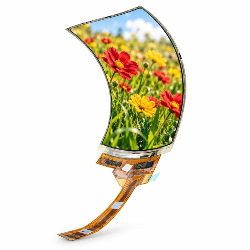
Flexible OLED Displays
Explore bendable or curvable display directions with mechanical limits reviewed for the assembly.
Explore product options →
Transparent OLED Displays
Explore see-through displays for showcases, signage and engineered commercial systems.
Explore product options →Project review
Review Your OLED Display Project
Send your application, content, size, interface, quantity and mechanical requirements. DisplayMan can review suitable OLED product options and distinguish module customization from new panel development.
Prefer to open the enquiry form here?
Technical References and Further Reading
- Canon Tokki: Manufacturing Process of OLED
- Samsung Display: OLED Cell
- Canon Tokki: Deposition and RGB Patterning
- Kateeva: Inkjet Printing Platform
- Universal Display: Organic Vapor Jet Printing
- Samsung Display: Quantum-Dot OLED Color Conversion
- Samsung Display: Thin Film Encapsulation
- Universal Display: Thin-Film Encapsulation
- Universal Display: Flexible OLEDs
This article provides a general manufacturing overview and practical OEM review questions. Process recipes and product limits belong to the qualified panel platform and approved module specification.